Low-Power ADC Custom ASIC (Fall 2012)
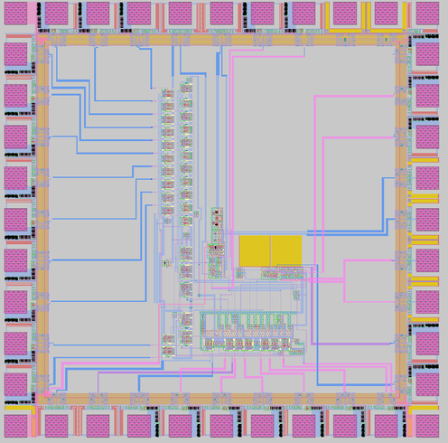
An integrated circuit design and layout based on the low-power ADC topology outlined in the thesis of EECS Ph.D graduate Heemin Yang titled "A Time-Based Energy Efficient Analog-to-Digital Converter". Several copies of the chip were manufactured and tested for performance.
The GoalMobile, embedded, and remote systems require the ability to run critical, high-performance operations for long durations of time. The available energy for such applications is often limited by size constraints, cost, or
inconvenience. Thus, the ability to design circuitry which can operate at low supply voltages and with little power consumption is critical for such applications. An important component in many such applications is an analog-to-digital converter (ADC), which allows for a digital processor to interpret real-world signals. The ProcessA low-power ADC was designed based on a hybrid dual slope-algorithmic ADC topology described here. Circuit operation and performance was simulated using LTSpice. A layout based on this design was created using the Magic 8.0 layout software. Several copies of the chip were manufactured using a MOSIS TSMC 0.35 micrometer process and tested for performance.
|
The SolutionA full description of our design and layout of the chip is provided in our final report. While the high-level circuit topology is described in the thesis, most implementation-level details (circuit design and layout) were determined independently by our team. Manufactured copies of the chip were tested by the team. Unfortunately, these chips did not function properly. We expect this to be a result of differences between the layout and the design. Though the design and layout circuit nets matched, parasitic effects in the layout likely altered the operation of the chip. Such problems could be overcome with additional layout experience.
My Responsibilities
|

